Project start: 2014-02-01
Project description: Use an STM32F4-DISCOVERY board with STM32F4DIS-BB and STM32F4DIS-LCD. Display some stuff. Use only datasheets and reference manuals; no existing code or examples.
I've got my eval boards and I've hooked everything up. First, I experimented with PWM output to the backlight control pin. Next I started setting up the FSMC for the parallel bus to the LCD controller. So far I'm seeing edges on the bus.
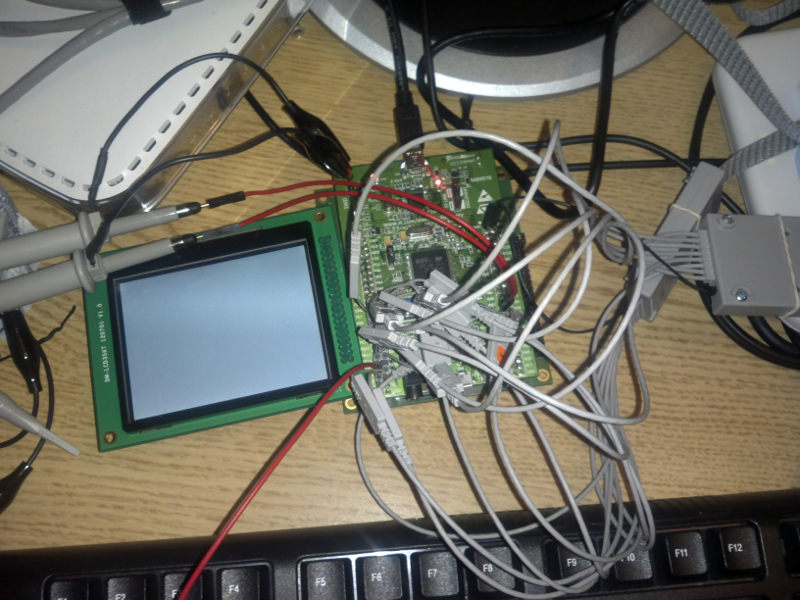
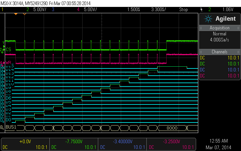
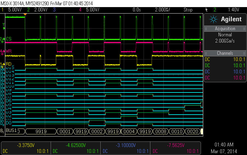
Today I've taken some scope captures of the parallel bus. I first did a walking 1's pattern to check that I had each of the digital probes connected correctly.
*(uint16_t*)0x60000000 = 0x1;
*(uint16_t*)0x60000000 = 0x2;
*(uint16_t*)0x60000000 = 0x4;
*(uint16_t*)0x60000000 = 0x8;
*(uint16_t*)0x60000000 = 0x10;
*(uint16_t*)0x60000000 = 0x20;
*(uint16_t*)0x60000000 = 0x40;
*(uint16_t*)0x60000000 = 0x80;
*(uint16_t*)0x60000000 = 0x100;
*(uint16_t*)0x60000000 = 0x200;
*(uint16_t*)0x60000000 = 0x400;
*(uint16_t*)0x60000000 = 0x800;
*(uint16_t*)0x60000000 = 0x1000;
*(uint16_t*)0x60000000 = 0x2000;
*(uint16_t*)0x60000000 = 0x4000;
*(uint16_t*)0x60000000 = 0x8000;
Looks good so far. I see a high level on the bits I expect when the Write Strobe is active (active low). We also see several bits that have blips when the strobe isn't active (D0, D3, D4, D8, D11, D12, and D15), which should probably be okay, though I'd prefer not to see them.
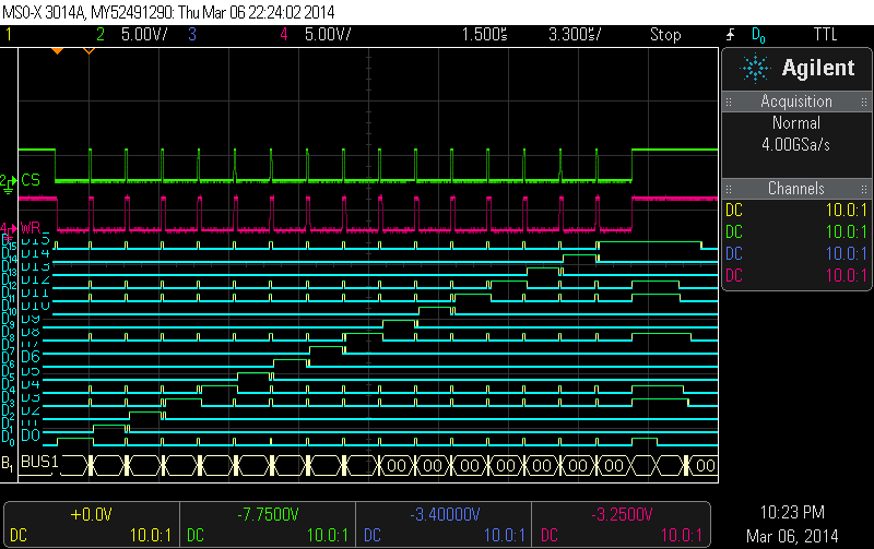
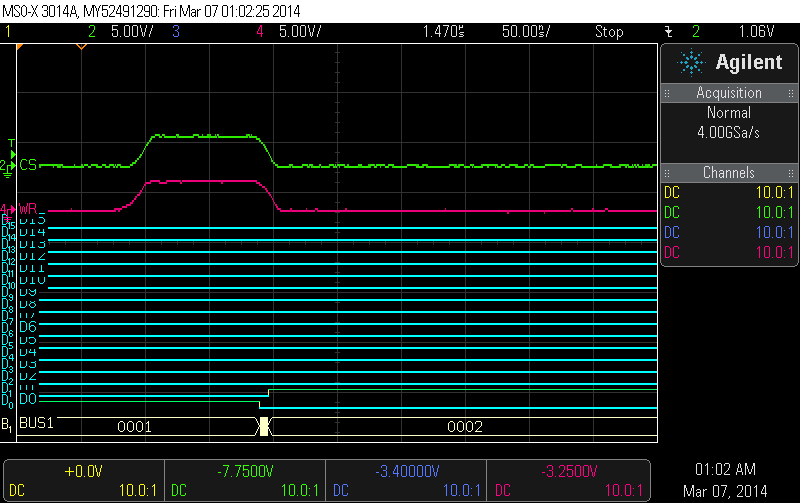
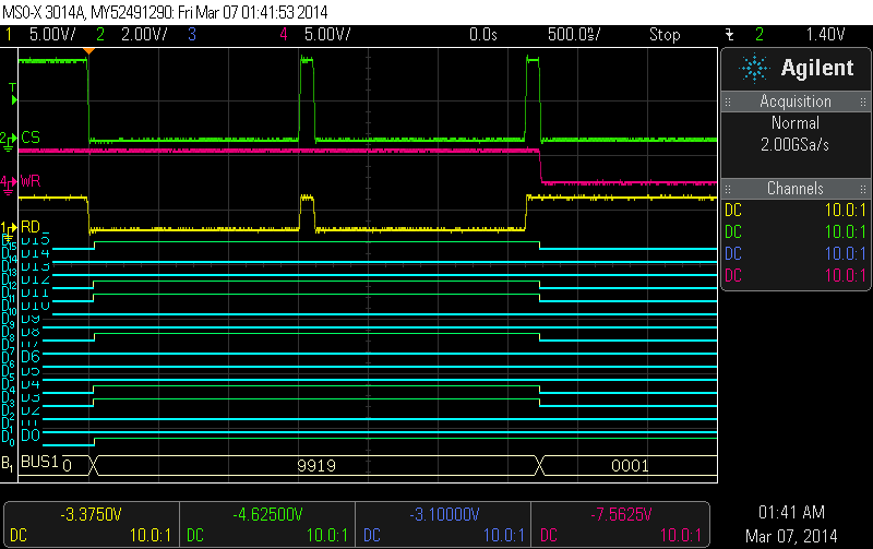
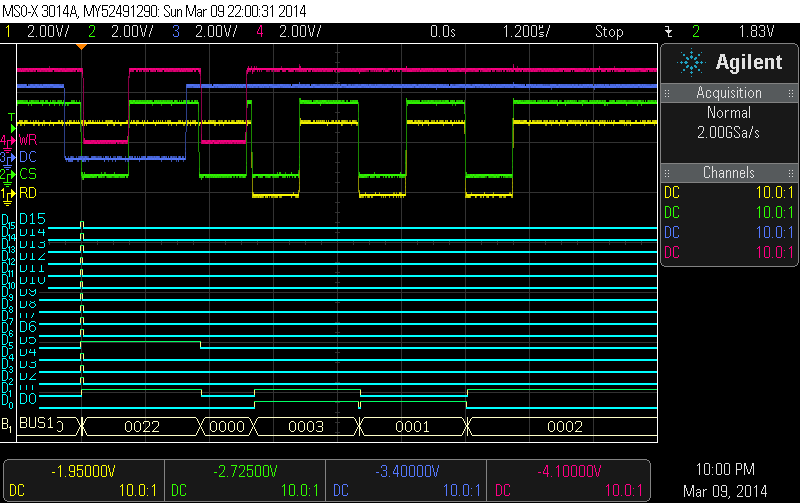
Lets look at a single byte transfer closer.
Looks like the data phase is going active exactly when the Write strobe kicks ("WR" on channel 4). D15 goes high when Chip Select ("CS" on channel 2) asserts before WR. Thereafter, several bits go high when CS and WR deassert, then all go low when CS asserts, and then the data arrives when WR asserts.
I'm a bit worried that the parallel data deasserts as WR and CS deassert. I don't know that the LCD controller won't pick up the data transition prior to the deassertion, or that it cares.
Note that I'm not using the default settings at the moment:
FSMC.bcr1 = (1 << 14) |
(1 << 12) |
(1 << 6) |
(1 << 4) |
(1 << 2) |
1;
This is Extended mode, Write Enable, Flash access, 16bit bus, NOR memtype, bank enable
What I really want (I think) is what is shown as "Mode 1" as shown in the STM32F07 reference manual. Unfortunately, most of my attempts result in my scope not even triggering. Further, some settings conflict. Case in point, Table 178 shows setting bits 31-20 of BTRx to 0, but bits 23-20 are the CLKDIV register, for which a value of 0 is reserved.
After trying several things, I started randomly changing settings. I finally got the following capture, which shows, I think, the CS and WR signals toggling beyond the bandwidth of my scope.
FSMC.bcr1 = (1 << 12) | (1 << 4) | (1 << 2) | 1;
FSMC.bwtr1 = (0 << 28) | (0xf << 24) | (1 << 20) | (0 << 16) | (4 << 8) | (1 << 4) | 0;
FSMC.btr1 = (0 << 28) | (0xf << 24) | (1 << 20) | (0 << 16) | (4 << 8) | (1 << 4) | 0;
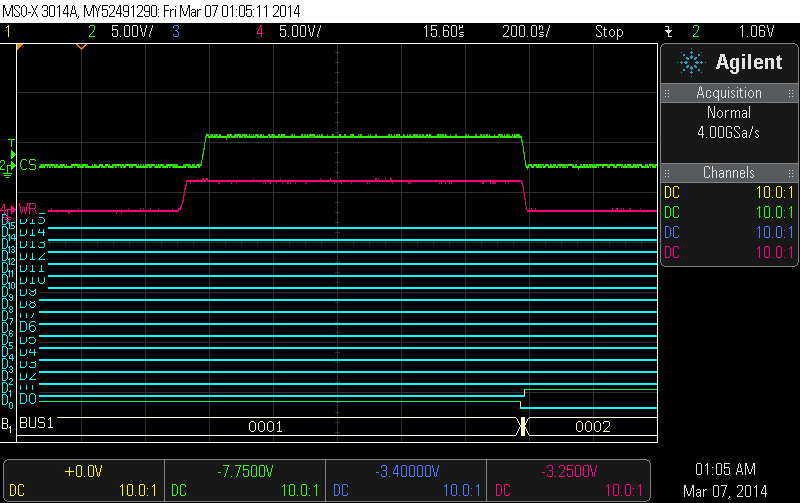
Updating the DATAST to 0xffff though looks pretty good, and now those glitchy things during CS/WR deassert are gone!
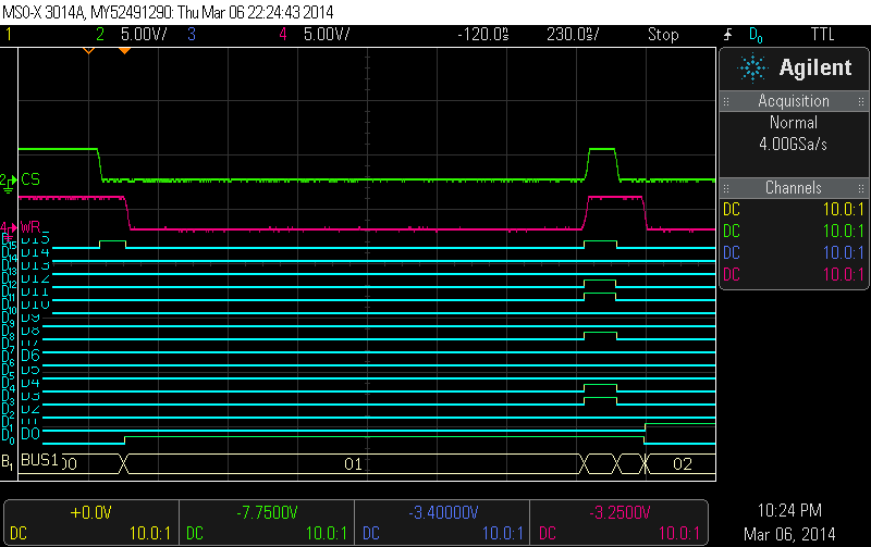
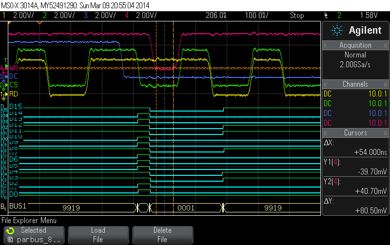
We are still in PSRAM mode instead of SRAM/ROM mode. While setting MTYPE to 0 before didn't work, it appears to now. Must have had a bad value somewhere in the BTR/BWTR registers. The good news is that WR is now rising before the data changes. The bad news is that is still rises with the chip select.
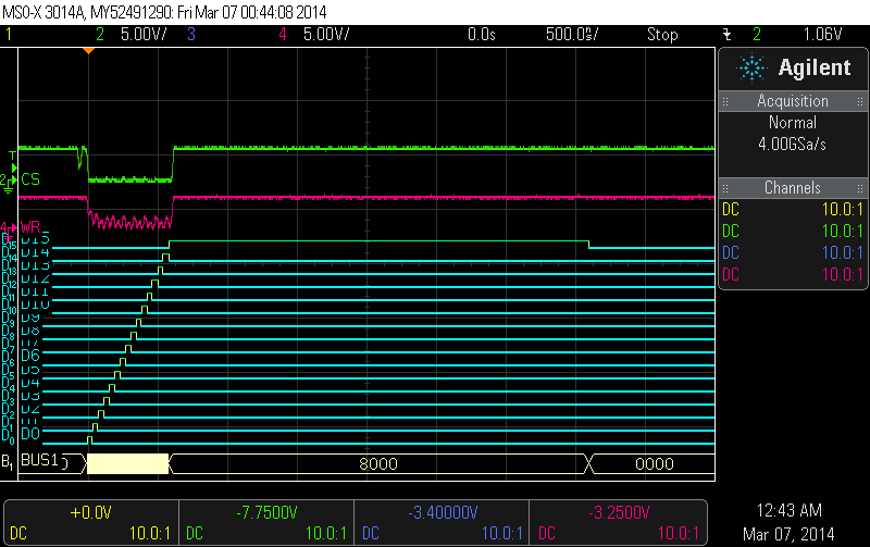
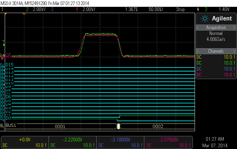
Looking very closely, it appears that WR actually deasserts ever so slightly before CS, though the edges overlap quite a bit. Of course, we are pretty much at the edge of my scope's capability. It might actually be clean. To see more clearly, I redo the capture, but with the MCU running at a slower speed. We can see that WR does in fact deassert first:
Next I tried to tighten the data duration a bit; not too fast but not the slowest. Unfortunately, after changing the delay from 0xffff to 0x1fff, I no longer get trigger. I changed it back to 0xffff, and still no trigger. Turns out a combination of too fast and not enough magnatude leads to this. First I put data on the bus in a never-ending while loop, and put the scope into autotrigger. I could see that the device wasn't idle, so I went back to normal trigger, and tried changing channel 2 from 2V per division to 5V per division (which trips a relay in the scope), and sure enough, it triggers again.
Setting the clkdiv doesn't seem to affect anything. I reduced the data duration to 0xff and increased the turnaround time to the max 0xf (so that I could still see the edges). With these settings, I placed the WR and CS signals nearly on top of each other to see the WR rise first at this speed.
There appears to be no way to increase the delay between Write deassert and CS deassert with this chip, so I'll stop messing with writes here. Time to move to reads!
So, lets do a couple back-to-back reads followed by a few reads interspersed with the writes.
Next up: Given 16 bit data bus, and no address bus and no address latch bit for interleave address/data, how do we address the LCD controller?
Embest (an Element 14 company) (maker of the STM32F4DIS-LCD board) distributes version 1.4 of the datasheet for the SSD2119 LCD controller. The controller appears to be a Solomon Systech chip. Solomon Systech does not freely distribute their datasheets. If you go on their website, the link for getting a datasheet takes you to a datasheet request page, where they want much personal info including your job title and for whom you work. I didn't bother submitting a request, neither wanting to wait for a response or worry that they'll ignore me as I'm not requesting this as part of my job.
In rev 1.4, there isn't a large ammount of good information as far as
bus timings go. For example, there is no timing diagram example for
the 8080 interface (which is the one Embest hard tied on the eval
board) Actually, there is no timing diagram in the beginning.
Section 13 has decent timing diagrams. In
section 7.1.2 "MPU Parallel 8080-serial Interface" they indicate that WR
latches write data and RD latches read data when CS is low (which follows
what we expect). It goes on to say that reading GDDRAM or reading the
status register is controlled by DC. No mention of what separates an
address phase vs a data phase.
To add further confusion, the SPI interface shows SDC (same pin as DC) to be low for specifying the register (address), and high for data.
It looks like they intermix "Command" and "Register". During the read phase earlier, we saw 9919 on the scope, which the datasheet indicates is the read value of the 0 command, that is, the device code. This looks promising. Now if we can just set a different address, say the oscillator address.
Thus far, the DC line has been high, and we know from our interleaved reads and writes that we always read back 0x9919, so DC being high must not be the address write (I'm guessing), which coincides with the SPI interface description so far.
A realization: the bits blips that occurred when CS was deasserted are that 9919 id for the LCD controller.
Today I'm going to review the timing diagram in the datasheet vs what I can scope. Then I will see if I can actually write to the device.
First up, the easy part: Address setup and hold times. The datasheet says they must be at least 0. Based on the timing diagram, this indicates that I needn't worry about the delays between CS, DC, and RW/RD. That is, they could rise and fall at the exact same time.
Next up: Pulse Widths. WR must be low for at least 40ns, then high for at least 20. With my current settings (mode B, 17 data latency, 16 clkdiv, 15 bus turnaround, 15 data duration (instead of 65535), 7 address hold and 7 address setup, the write pulse width is low about 54ns, then CS is high for about 74ns.
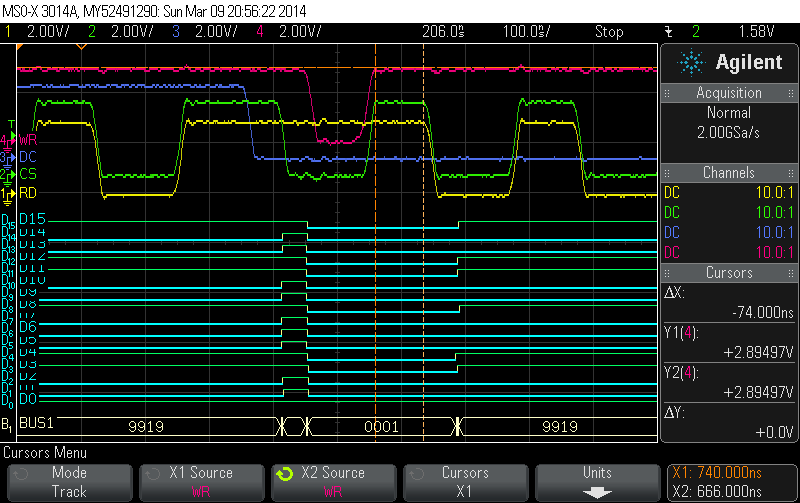
Of course, these edges are quite rounded by the limits of my scope.
Data setup and hold are similarly good. Setup is 5ns, but appears on our digital capture just before WR falls. Data hold is measured after WR rises, and must be at least 5ns. We hold through the duration of the CS deassert, so no problem there.
That's the end of the write timings, and they look good. So, on to the reads.
The pulse width requirements are MUCH larger for reads. Same for the setup and hold. Low followed by high must be a full 500ns. At the low edge of RD, the access time (delay until valid data) is a full 250ns. At the rising edge of RD, the device has an output hold of 100ns (which seems to extend beyond the end of the data valid section.
Making the data duration longer is no problem; I can set it to 255 to meat the low pulse width and data access times. The high pulse width is much more challenging. At the maximum bus turn around time only gives me about 90ns of the 500 required.
To work around this; I'll add a software delay to every read transaction. Unfortunately, I still seem to always read back 0x9919.
... an hour passes... I look attempt to just go through the motions for initializing the device, and amazingly, I get a display full of random colors. I then looped on writing the 0x22 register and I got a pattern on (most of) the screen. I then looked through the register descriptions, and realized something: The only registers listed for read access are the ident code and register 0x22! I tried reading register 22, and amazingly, it looks like that works:
And here is what the screen looks like at the moment:
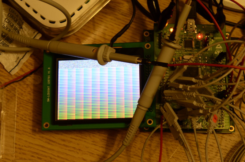
It still flickers quite a bit. Setting the FLD bit helps quite a bit.
After playing with a few patterns, I thought I should start working on making images. However, I have run into a problem. In 16 bit color mode, storing pixel values for the screen in RAM would consume 153600 bytes (150 kiB). This is a problem since this microcontroller only has 112 kiB of contiguous memory. Reducing to 8bit color still consumes 75kiB, and my linker currently doesn't like that either. Actually displaying useful stuff will have to wait for another day.